- 您现在的位置:买卖IC网 > Sheet目录3855 > PIC16C62B-20/SS (Microchip Technology)IC MCU OTP 2KX14 PWM 28SSOP
PIC16C62B/72A
1999 Microchip Technology Inc.
Preliminary
DS35008B-page 37
7.3.3
SET-UP FOR PWM OPERATION
The following steps should be taken when configuring
the CCP module for PWM operation:
1.
Set the PWM period by writing to the PR2 regis-
ter.
2.
Set the PWM on-time by writing to the CCPR1L
register and CCP1CON<5:4> bits.
3.
Make the CCP1 pin an output by clearing the
TRISC<2> bit.
4.
Set the TMR2 prescale value and enable Timer2
by writing to T2CON.
5.
Configure the CCP1 module for PWM operation.
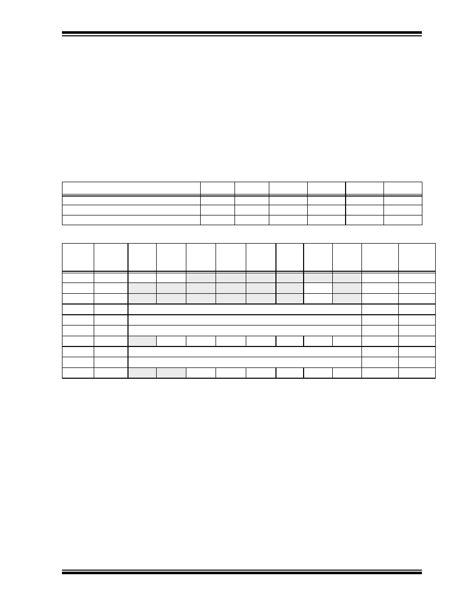
TABLE 7-4
EXAMPLE PWM FREQUENCIES AND RESOLUTIONS AT 20 MHz
TABLE 7-5
REGISTERS ASSOCIATED WITH PWM AND TIMER2
PWM Frequency
1.22 kHz
4.88 kHz
19.53 kHz
78.12 kHz
156.3 kHz
208.3 kHz
Timer Prescaler (1, 4, 16)
16
4
1
PR2 Value
0xFF
0x3F
0x1F
0x17
Maximum Resolution (bits)
10
8
7
5.5
Address
Name
Bit 7
Bit 6
Bit 5
Bit 4
Bit 3
Bit 2
Bit 1
Bit 0
Value on
POR,
BOR
Value on
all other
resets
0Bh,8Bh
INTCON
GIE
PEIE
T0IE
INTE
RBIE
T0IF
INTF
RBIF
0000 000x 0000 000u
0Ch
PIR1
—
ADIF
—
SSPIF
CCP1IF
TMR2IF
TMR1IF
-0-- 0000 -0-- 0000
8Ch
PIE1
—
ADIE
—
SSPIE
CCP1IE
TMR2IE
TMR1IE
-0-- 0000 -0-- 0000
87h
TRISC
PORTC Data Direction Register
1111 1111 1111 1111
11h
TMR2
Timer2 module’s register
0000 0000 0000 0000
92h
PR2
Timer2 module’s period register
1111 1111 1111 1111
12h
T2CON
—
TOUTPS3 TOUTPS2 TOUTPS1 TOUTPS0 TMR2ON T2CKPS1 T2CKPS0 -000 0000 -000 0000
15h
CCPR1L
Capture/Compare/PWM register1 (LSB)
xxxx xxxx uuuu uuuu
16h
CCPR1H
Capture/Compare/PWM register1 (MSB)
xxxx xxxx uuuu uuuu
17h
CCP1CON
—
CCP1X
CCP1Y
CCP1M3 CCP1M2 CCP1M1 CCP1M0 --00 0000 --00 0000
Legend:
x
= unknown, u = unchanged, - = unimplemented read as '0'. Shaded cells are not used by PWM and Timer2.
发布紧急采购,3分钟左右您将得到回复。
相关PDF资料
PIC16LC711-04I/SO
IC MCU OTP 1KX14 A/D 18SOIC
PIC18F66J90-I/PT
IC PIC MCU FLASH 64KB 64-TQFP
ATMEGA32L-8AC
IC AVR MCU 32K LV 8MHZ COM44TQFP
DSPIC30F2012-30I/SP
IC DSPIC MCU/DSP 12K 28DIP
PIC18LF2321-I/ML
IC PIC MCU FLASH 4KX16 28QFN
PIC18F4321-I/P
IC PIC MCU FLASH 4KX16 40DIP
ATMEGA32L-8MC
IC AVR MCU 32K LV 8MHZ COM 44QFN
PIC18F2450-I/SP
IC PIC MCU FLASH 8KX16 28DIP
相关代理商/技术参数
PIC16C62B-20E/SO
功能描述:8位微控制器 -MCU 3.5KB 128 RAM 22 I/O RoHS:否 制造商:Silicon Labs 核心:8051 处理器系列:C8051F39x 数据总线宽度:8 bit 最大时钟频率:50 MHz 程序存储器大小:16 KB 数据 RAM 大小:1 KB 片上 ADC:Yes 工作电源电压:1.8 V to 3.6 V 工作温度范围:- 40 C to + 105 C 封装 / 箱体:QFN-20 安装风格:SMD/SMT
PIC16C62B-20E/SP
功能描述:8位微控制器 -MCU 3.5KB 128 RAM 22 I/O RoHS:否 制造商:Silicon Labs 核心:8051 处理器系列:C8051F39x 数据总线宽度:8 bit 最大时钟频率:50 MHz 程序存储器大小:16 KB 数据 RAM 大小:1 KB 片上 ADC:Yes 工作电源电压:1.8 V to 3.6 V 工作温度范围:- 40 C to + 105 C 封装 / 箱体:QFN-20 安装风格:SMD/SMT
PIC16C62B-20E/SS
功能描述:8位微控制器 -MCU 3.5KB 128 RAM 22 I/O RoHS:否 制造商:Silicon Labs 核心:8051 处理器系列:C8051F39x 数据总线宽度:8 bit 最大时钟频率:50 MHz 程序存储器大小:16 KB 数据 RAM 大小:1 KB 片上 ADC:Yes 工作电源电压:1.8 V to 3.6 V 工作温度范围:- 40 C to + 105 C 封装 / 箱体:QFN-20 安装风格:SMD/SMT
PIC16C62B-20I/ML
功能描述:8位微控制器 -MCU 3.5KB 128 RAM 22 I/O RoHS:否 制造商:Silicon Labs 核心:8051 处理器系列:C8051F39x 数据总线宽度:8 bit 最大时钟频率:50 MHz 程序存储器大小:16 KB 数据 RAM 大小:1 KB 片上 ADC:Yes 工作电源电压:1.8 V to 3.6 V 工作温度范围:- 40 C to + 105 C 封装 / 箱体:QFN-20 安装风格:SMD/SMT
PIC16C62B-20I/SO
功能描述:8位微控制器 -MCU 3.5KB 128 RAM 22 I/O RoHS:否 制造商:Silicon Labs 核心:8051 处理器系列:C8051F39x 数据总线宽度:8 bit 最大时钟频率:50 MHz 程序存储器大小:16 KB 数据 RAM 大小:1 KB 片上 ADC:Yes 工作电源电压:1.8 V to 3.6 V 工作温度范围:- 40 C to + 105 C 封装 / 箱体:QFN-20 安装风格:SMD/SMT
PIC16C62B-20I/SO
制造商:Microchip Technology Inc 功能描述:8BIT CMOS MCU SMD 16C62 SOIC28
PIC16C62B-20I/SP
功能描述:8位微控制器 -MCU 3.5KB 128 RAM 22 I/O RoHS:否 制造商:Silicon Labs 核心:8051 处理器系列:C8051F39x 数据总线宽度:8 bit 最大时钟频率:50 MHz 程序存储器大小:16 KB 数据 RAM 大小:1 KB 片上 ADC:Yes 工作电源电压:1.8 V to 3.6 V 工作温度范围:- 40 C to + 105 C 封装 / 箱体:QFN-20 安装风格:SMD/SMT
PIC16C62B-20I/SP
制造商:Microchip Technology Inc 功能描述:IC 8BIT CMOS MCU 16C62 SDIL28